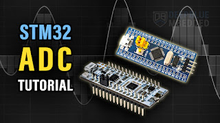
How to program new STM32F205RET6 MCU?
Here’s a practical, no-nonsense guide to get a brand-new STM32F205RET6 (512 KB Flash, LQFP-64) up and programmable.
1) Minimal hardware you must have (or it won’t run)
-
Power
-
VDD pins → 3.3 V, each VDD/VSS pair gets a 0.1 µF ceramic right at the pins.
-
Add one 4.7–10 µF bulk cap near the MCU.
-
VDDA → 3.3 V via small RC (e.g., 10 Ω + 1 µF) or at least a 0.1 µF; VSSA → GND.
-
VBAT tie to 3.3 V (or a battery if you need RTC backup).
-
-
Internal regulator caps (mandatory on F2):
-
VCAP1, VCAP2 → 2.2 µF low-ESR ceramics to GND (these are NOT supply pins; they must have caps or the core won’t start).
-
-
Reset / Boot
-
NRST pull-up 10 kΩ → 3.3 V (optional 100 nF to GND for extra robustness).
-
BOOT0 pull-down 100 kΩ → GND (normal “boot from Flash”).
-
BOOT1 is on PB2 (leave low/default unless you need special modes).
-
-
Clock
-
You can start on HSI (internal)—no crystal required.
-
If you want USB or tighter timing later, add an HSE crystal (e.g., 8–12 MHz) with proper load caps.
-
2) Easiest programming path: SWD with ST-LINK
Pins to break out (LQFP-64):
-
SWDIO = PA13
-
SWCLK = PA14
-
NRST
-
GND
-
3.3 V (target power or at least a VTref sense for the probe)
Hookup
-
ST-LINK/V2-1 (or V2) → your board
-
ST-LINK SWDIO → PA13
-
ST-LINK SWCLK → PA14
-
ST-LINK NRST → NRST
-
ST-LINK GND → GND
-
ST-LINK 3.3 V (VTref) → 3.3 V on your board
-
Flashing
-
Power the board (stable 3.3 V).
-
Open STM32CubeProgrammer (or use STM32CubeIDE).
-
Interface: SWD, click Connect.
-
Full chip erase (first time), then Program your .hex/.elf.
-
Check Option Bytes:
-
RDP = Level 0 (unlocked)
-
Keep SWD enabled (don’t disable JTAG/SWD until you’re sure).
-
Tip: Don’t reassign PA13/PA14 in firmware unless you know how to recover. If you lock yourself out, set BOOT0 = 1 and use the ROM bootloader (next section) to re-flash.
3) No debugger? Use the built-in system bootloader
The ROM bootloader supports multiple peripherals on F2 parts:
-
USART (common, simple)
-
USB FS (DFU) (needs USB connector on PA11/PA12)
-
(Also CAN on some variants; most folks use USART/USB)
Enter system bootloader
-
Pull BOOT0 = 1 (to 3.3 V), keep BOOT1(PB2) = 0, then reset.
-
MCU boots from System Memory (ROM loader).
USART example (simple FTDI/CP2102)
-
Wire MCU TX/RX to USB-UART:
-
PA9 = USART1_TX, PA10 = USART1_RX (also can use USART2 PA2/PA3, USART3 PB10/PB11)
-
Cross-connect TX↔RX, plus GND.
-
-
In STM32CubeProgrammer, pick UART, select COM port, connect at 115200 (start slower if needed), then erase/program.
USB DFU example
-
Add USB micro-B: PA12 (DP), PA11 (DM), proper ESD protection and routing.
-
With BOOT0=1, connect to PC → device appears as DFU.
-
Use CubeProgrammer (USB) or dfu-util to flash.
4) First firmware checklist (CubeMX/CubeIDE)
-
Create project for STM32F205RETx.
-
RCC: start with HSI; add PLL later.
-
Enable SYS → Debug = Serial Wire.
-
If using UART console: enable USART1 on PA9/PA10 (115200 8N1).
-
Generate code, build, flash via SWD.
Test with a blinky on any GPIO (e.g., PA5) to confirm clocks/run.
5) Common pitfalls (save hours)
-
Missing VCAP caps → CPU won’t start. Add 2.2 µF on both VCAP1 & VCAP2.
-
No decoupling on VDD/VDDA → random resets or connection failures.
-
BOOT0 floating → unpredictable boots. Add that 100 kΩ pulldown.
-
SWD disabled by code → can’t connect. Recover with BOOT0=1 (system bootloader), then re-flash.
-
Wrong target voltage in ST-LINK → no connection; VTref must match 3.3 V.
-
USB DFU not seen → you need the USB connector + proper pins and BOOT0=1 (or run your own DFU firmware).
6) Quick pin recap (LQFP-64 highlights)
-
SWD: PA13 (SWDIO), PA14 (SWCLK), NRST
-
USART1: PA9 (TX), PA10 (RX)
-
USB FS: PA11 (DM), PA12 (DP)
-
BOOT0: dedicated pin (pull-down 100 kΩ)
-
BOOT1: PB2
-
VCAP1/2: 2.2 µF to GND (mandatory)
TL;DR
-
Put the right caps on VCAP1/2 and VDD/VDDA.
-
Tie BOOT0 → GND (100 kΩ) for normal boot.
-
Break out SWD (PA13/PA14/NRST) and program with ST-LINK via STM32CubeProgrammer.
-
Alternatively, set BOOT0=1 and use USART/USB DFU ROM bootloader to flash.


评论
发表评论