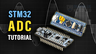
How to allocate schematic IO for STM32?
Allocating Schematic I/O for STM32 Microcontrollers
When designing a schematic for an STM32 microcontroller, careful I/O allocation ensures proper functionality, ease of debugging, and flexibility for future modifications.
1. Identify Key Design Requirements
Before assigning I/O pins, consider:
- Peripherals Needed: UART, SPI, I2C, CAN, ADC, PWM, etc.
- Power Supply and Reset: VCC, GND, NRST, BOOT0 pins.
- Communication Interfaces: External components such as sensors, displays, memory, etc.
- Debugging & Programming: SWD/JTAG interface.
- GPIO Functionality: Digital inputs, outputs, interrupts, etc.
2. Pin Allocation Process
A. Use STM32CubeMX for Pin Configuration
STM32CubeMX is an official tool from STMicroelectronics that helps visually configure pins and generate initialization code.
- Select STM32 MCU model.
- Enable required peripherals.
- Assign I/O pins and check conflicts.
- Generate C code for initialization.
B. Power and Ground Pins
- VDD & VSS: Connect all power pins to 3.3V and GND.
- VSSA & VDDA: Power for analog peripherals (ADC, DAC). Add LC filter for noise reduction.
- Decoupling Capacitors: Place 100nF capacitors close to each VDD pin.
C. Reset & Boot Configuration
- NRST Pin:
- Connect a 10kΩ pull-up resistor.
- Add a 100nF capacitor to ground for stable reset.
- BOOT0 Pin:
- Pull LOW (GND) for normal execution.
- Pull HIGH (VDD) for DFU/Bootloader mode (firmware updates via USB/UART).
D. Debug & Programming Interface
- SWD (Serial Wire Debug, recommended)
- SWCLK → Connect to debugger.
- SWDIO → Connect to debugger.
- NRST → Optional for reset during debugging.
- Pull-up 100kΩ on SWDIO.
- JTAG (For advanced debugging, not always needed)
- Uses TCK, TMS, TDI, TDO, NRST.
E. Peripheral Pin Allocation
1. UART (For Serial Communication)
- TX & RX: Assign to UARTx.
- Optional RTS/CTS: If using hardware flow control.
2. I2C (For Sensors, EEPROM, Displays)
- SCL & SDA: Assign to I2Cx.
- Pull-up resistors (4.7kΩ or 10kΩ) required on SCL and SDA.
3. SPI (For Flash, Sensors, Displays)
- SCK, MISO, MOSI, NSS: Assign to SPIx.
- Pull-up on NSS if software-controlled.
4. CAN (For Automotive, Industrial Applications)
- CAN_RX & CAN_TX: Assign to CANx.
- Requires CAN Transceiver (e.g., MCP2551, TJA1050).
5. ADC (For Analog Sensors, Voltage Measurement)
- Choose ADCx_INy pins.
- Connect sensors with proper filter capacitors.
- VDDA must be stable for ADC accuracy.
6. PWM / Timers (For Motor Control, LED Dimming)
- Assign TIMx_CHy to PWM output pins.
- Ensure correct timer selection in STM32CubeMX.
3. Example Schematic Pinout (STM32F103C8T6)
| Function | Pin | Notes |
|---|---|---|
| Power | VDD, VSS | Connect all power pins |
| Reset | NRST | 10kΩ pull-up, 100nF capacitor |
| Debugging | SWCLK, SWDIO | SWD programming |
| UART1 | PA9 (TX), PA10 (RX) | Serial Communication |
| I2C1 | PB6 (SCL), PB7 (SDA) | 4.7kΩ pull-ups required |
| SPI1 | PA5 (SCK), PA6 (MISO), PA7 (MOSI) | NSS (Optional) |
| ADC | PA0 (ADC_IN0) | Analog sensor input |
| PWM | PA8 (TIM1_CH1) | Motor or LED control |
4. Best Practices
- Use STM32CubeMX to avoid pin conflicts.
- Group related signals (UART, I2C, etc.) for easy routing.
- Reserve unused GPIOs for future features.
- Check electrical characteristics (voltage, current limits).
- Minimize cross-talk between high-speed and analog signals.
Conclusion
Allocating I/O for an STM32 schematic requires planning for power, debugging, communication, and peripheral interfaces. Using STM32CubeMX simplifies pin selection and avoids conflicts. Proper design ensures a reliable and scalable hardware system.
.gif)


评论
发表评论